

Beyond Silicon.
Customer value first
Pursuit of absolute quality
Leading innovative technologies
Differentiated technology and industry-leading expertise
Precision matters.
World-class competitiveness based on
differentiated technology and industry-leading expertise

Environmental.
Social.
Governance.

Why Invest in HANA Materials?

Be original.
Challenging and creative talent,
you are the protagonist of HANA Materials.
Precision matters
World-class competitiveness based on
differentiated technology and industry-leading expertise
Silicon
HANA Materials, growing with technology and future, We will head toward the customer-centric management for Silicon products.
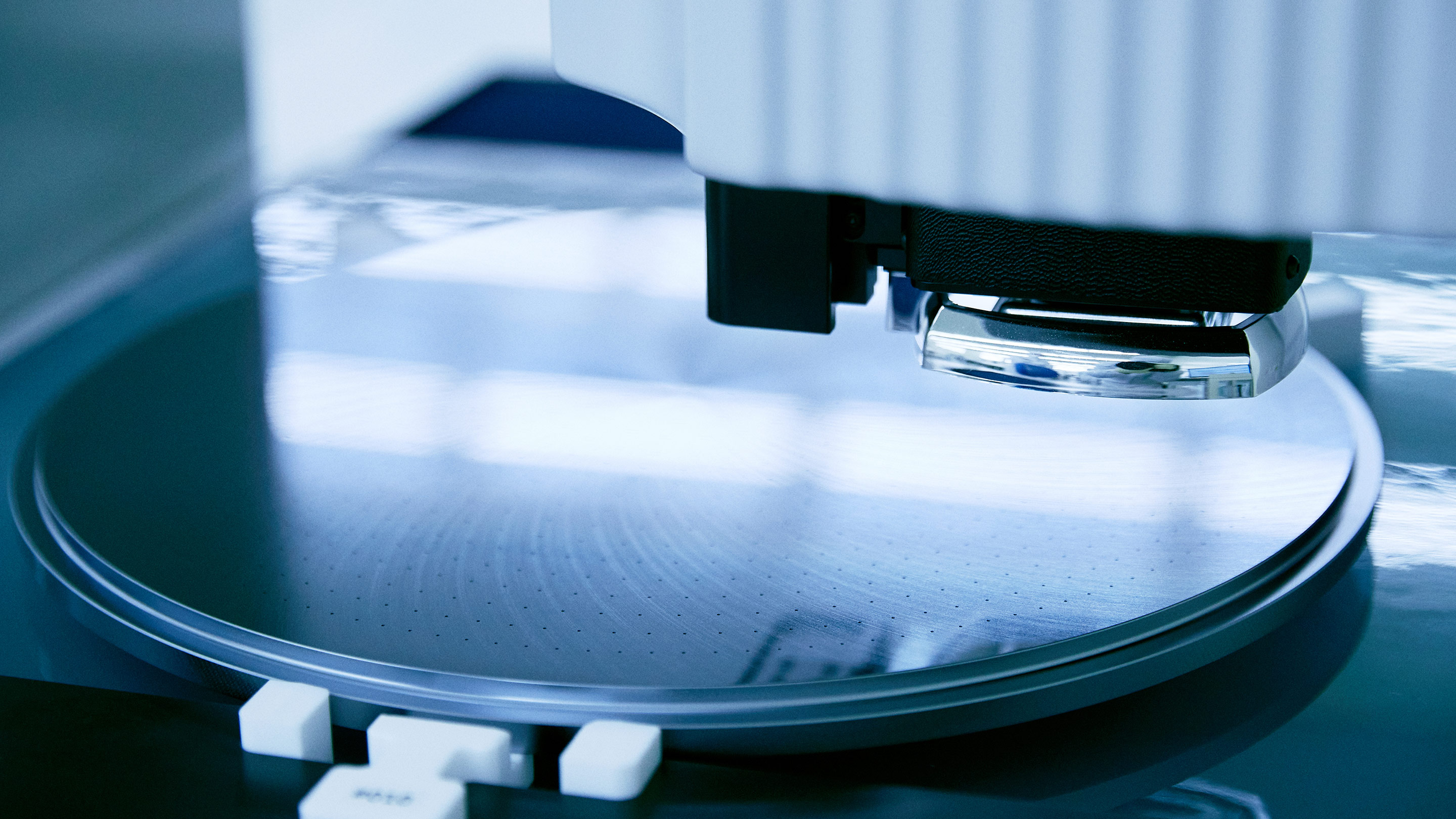
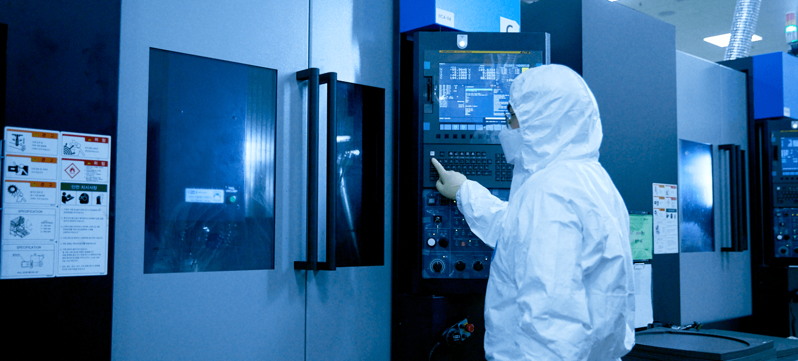
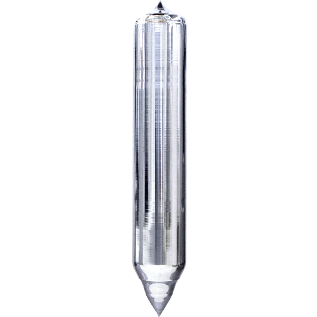
Silicon is a dark gray-colored metallic substance with the chemical symbol, “Si”. Silicon used in semiconductor process is monocrystalline silicon which is ultra-high pure metal silicon that is three dimensionally well-organized.
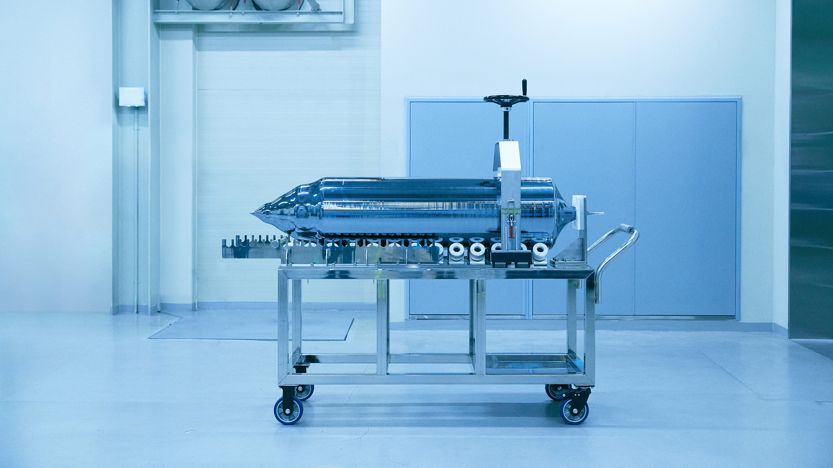
We, as a company that internally possesses core technology including the design of Hot Zone (polysilicon melting furnace) which is the core parts of ingot growing facilities and growth factor optimization developed the ingot with more than 520mm of diameter, for the first time in South Korea.
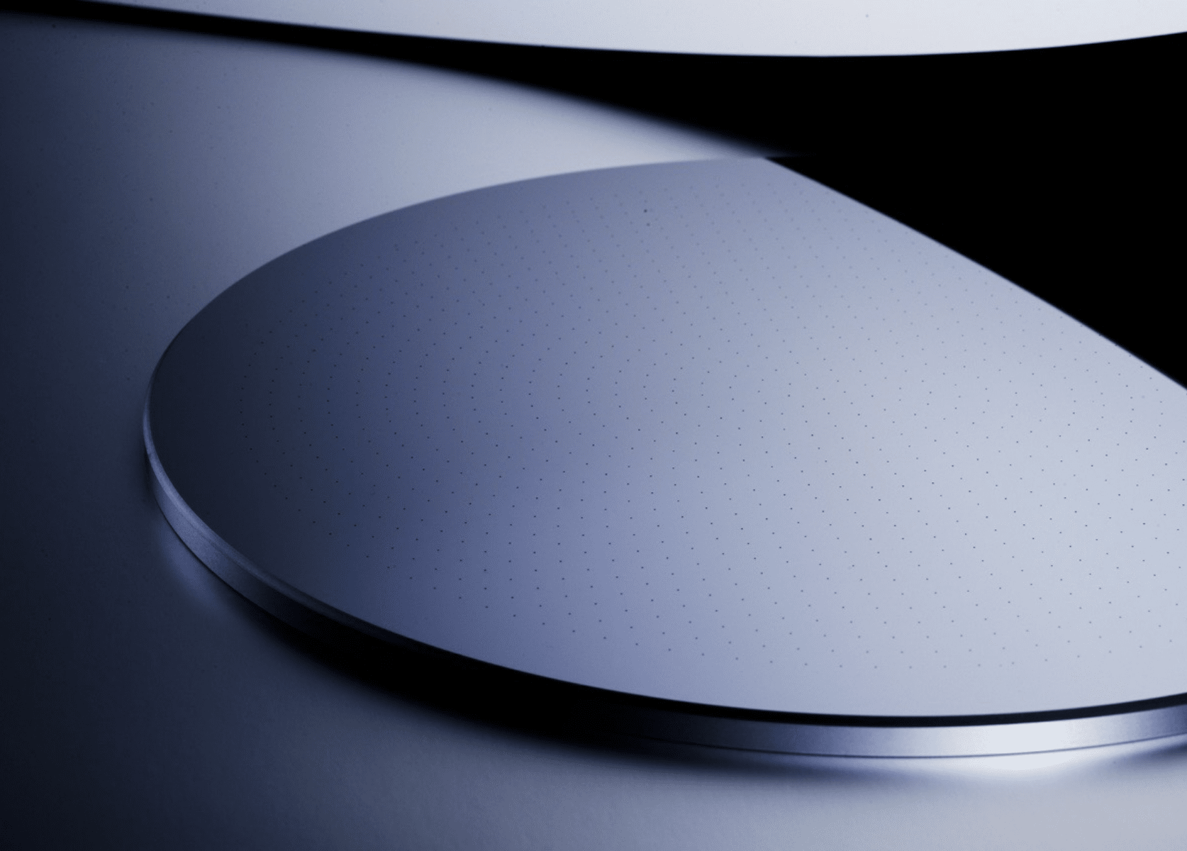
Specification
Properties
Value
Material
Single Crystal Silicon
Out diameter
550mm ~ 240mm
Resistivity(Ω.㎝)
Low Res. (< 0.02)
Middle Res. (1~4)
High Res. (60~90)
RRG < 5%
< 5%
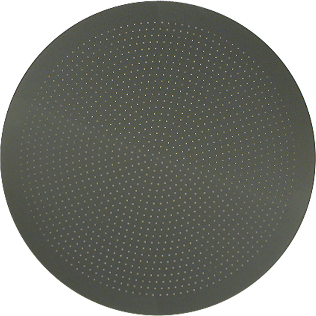
Gas hole
Diameter 0.8~0.2mm
Roundness < 0.02mm
Concentricity < 0.02mm
Δ XY-Position < 0.05mm
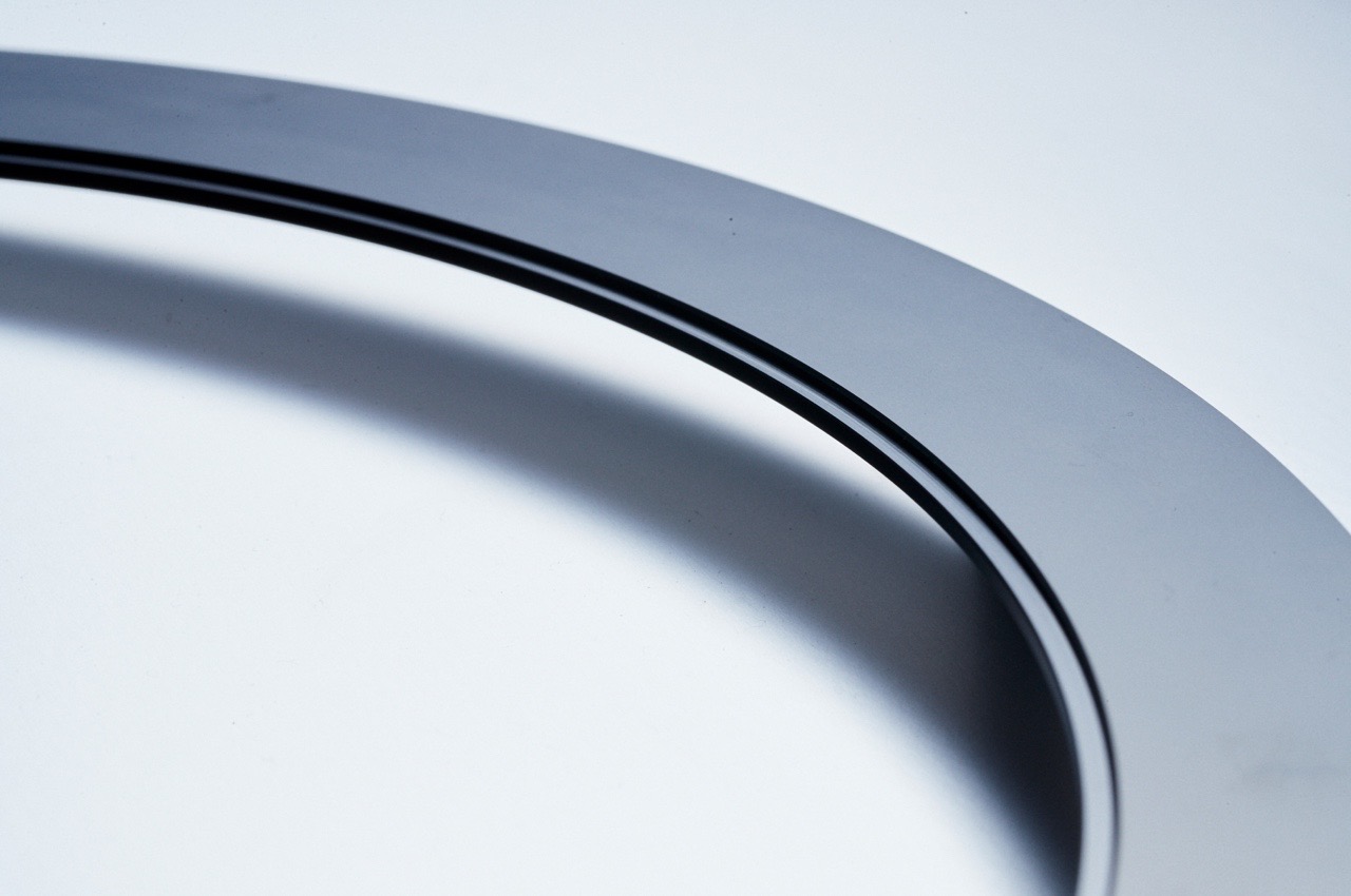
Surface condition
Polishing, Lapping, Grinding
Surface Flatness
< 10 ㎛
Machining precision
< 10 ㎛
Quality
Chipping, Scratch, Crack free
Contamination, Stain free

Specification
Properties
Value
Material
Single Crystal Silicon
Multi Crystal Silicon
Out diameter
580mm ~ 240mm
Resistivity(Ω.㎝)
Low Res. (< 0.02)
Middle Res. (1~4)
High Res. (60~90)
RRG < 5%
< 5%
Surface condition
Polishing, Lapping, Grinding
Surface Flatness
< 10 ㎛
Machining precision
< 15 ㎛
Quality
Chipping, Scratch, Crack free
Contamination, Stain free
Specification
Properties
Single Crystal Ingot
Multi-Crystalline “Poly” Ingot
Purity (%)
> 8N
> 6N
Diameter / Size (mm)
300~600
980*980*280
Type/Doped
P,N/Boron,Phosphorus
P/Boron
Resistivity (Ω.cm)
Low Res. (< 0.02)
Middle Res. (1~4)
High Res. (60~90)
Middle Res. (1~4)
RRG (%)
< 5
< 8
Oxygen concentration (ppma)
≤ 13
≤ 20
Carbon concentration (ppma)
≤ 0.5
≤ 1
Sitemap
Links
HANA MICRON
HANA Materials Inc. /
50, 3gongdan 3-ro, Seobuk-gu, Cheonan-si, Chungcheongnam-do / TEL 041-410-1015
Copyright (c) 2022 HANA Materials Inc. All Rights Reserved.